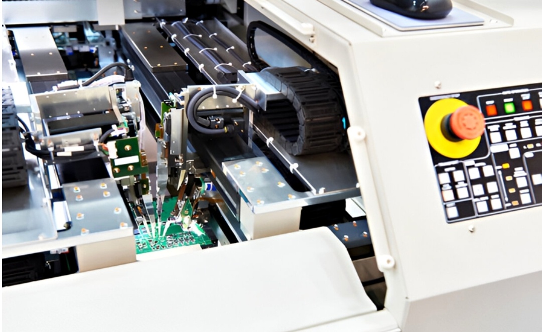
A VIPPO PCB has become one of the most essential technologies in modern electronics manufacturing, especially for devices that require high-density layouts, strong solder joints, and reliable thermal performance. VIPPO stands for Via-In-Pad Plated Over, a process in which vias are drilled directly into the pad, plated, filled, and sealed. Unlike traditional via structures, where vias are kept outside the component pad, the VIPPO technique integrates the via directly within the component’s land area. This creates a compact, high-strength, and electrically stable interconnection method that is vital for advanced electronic assemblies.
As electronics continue to shrink in size but increase in performance expectations, the demand for VIPPO PCB technology has grown rapidly. This layout method is extremely valuable for fine-pitch BGA packages, microcontrollers, network processors, RF modules, high-speed communication circuits, and other applications where board space is limited and signal integrity is crucial.
What Makes a VIPPO PCB Different
The biggest distinction of a VIPPO PCB is its ability to allow vias to be located directly inside the component pads. After drilling, the via is plated, filled with conductive or non-conductive epoxy, and then over-plated with copper to create a perfectly flat surface. This pad structure supports stable component soldering without the risk of solder wicking into the via hole.
A properly executed VIPPO structure maintains uniform flatness across all pads, which is especially important for BGA and QFN components. Without flatness, solder joints may not form correctly, causing open joints, shifting, or tombstoning. With VIPPO, the top layer surface becomes smooth and consistent, enhancing both mechanical and electrical performance.
Why VIPPO PCB Technology Has Become Essential
The rising complexity of electronics requires more efficient use of PCB real estate. Adding more components while reducing board size means that traditional via placement strategies often create routing limitations. VIPPO provides the perfect solution for high-density design because vias within pads free up routing channels, enabling cleaner and more efficient layout patterns.
Additionally, the thermal and electrical advantages are significant. Since the via is directly under the component, heat dissipation improves substantially. The electrical path is shorter and more stable, which is critical for low-noise, high-frequency, and high-current circuits. This makes a VIPPO PCB especially valuable in advanced communication systems, industrial control units, consumer electronics, medical equipment, aerospace electronics, and automotive technology.
Manufacturing Process of a VIPPO PCB
The production of a VIPPO PCB requires advanced fabrication capabilities and highly controlled processes. It starts with drilling microvias into the exact pad locations. After drilling, plating takes place to create a conductive via wall. The next step involves filling the via using a specialized resin or conductive epoxy. This filled area must be perfectly flat and void-free.
Once the filling cures, copper plating is applied over the pad, creating a flush and uniform surface. The PCB then goes through the standard etching, lamination, imaging, solder mask, and surface finish processes. Since each step must be executed with precision, manufacturers that produce VIPPO designs must adhere to strict tolerances and quality control procedures.
Performance Benefits of a VIPPO PCB
A VIPPO PCB provides distinct performance improvements over conventional designs. Because the via sits directly under the component, the electrical performance improves through reduced inductance and resistance. Signal integrity becomes stronger, especially in high-frequency applications such as RF systems and high-speed digital designs. VIPPO structures also deliver consistent solder joints, reducing the risk of solder voids or insufficient wetting.
Thermal management improves significantly because heat can travel through the via more efficiently. This is vital for high-power devices such as LED drivers, motor controllers, and communication processors. Additionally, overall board reliability increases because VIPPO reduces mechanical stress on solder joints by reinforcing the pad area. The stronger pad foundation limits solder cracking and improves long-term reliability.
Applications Where VIPPO PCB Offers the Most Value
The versatility of VIPPO makes it suitable for countless industries. Telecommunications companies rely on VIPPO designs for routers, repeaters, base stations, and fiber-optic components. In the automotive sector, electric vehicle controllers, power modules, and sensors frequently use VIPPO to achieve compact, high-performance layouts. Consumer electronics such as smartphones, gaming devices, and wearables depend on VIPPO to support fine-pitch, high-speed chips.
Industrial automation, robotics, aerospace systems, defense electronics, and medical devices also benefit enormously from the stability and durability offered by VIPPO PCB technology. In every case, the technology supports safe, efficient, and long-lasting circuit performance.
Conclusion: Choose the Right Partner for Premium VIPPO PCB Manufacturing
A VIPPO PCB offers unmatched advantages in reliability, performance, heat management, and high-density design. It supports the growing demand for compact, powerful, and thermally efficient electronics across all major industries. However, the success of a VIPPO board depends entirely on the precision and expertise of the manufacturer. If you want flawless results for prototypes, small batches, or large-scale production, the best approach is to work with an experienced VIPPO PCB Manufacturer that understands this advanced fabrication technology and follows strict engineering and quality control standards.

